
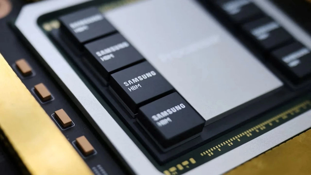
Samsung Electronics has unveiled an ambitious new vision for the future of High Bandwidth Memory (HBM) technology at the prestigious Hot Chips symposium, signaling a fundamental shift in how memory components will function within artificial intelligence systems. The South Korean technology giant announced plans to transform the base die of HBM stacks from a simple interconnect layer into a fully functional computing component, potentially revolutionizing the architecture of next-generation AI accelerators.
This strategic pivot represents Samsung’s response to the explosive growth in AI computing demands, where traditional memory architectures increasingly struggle to keep pace with the computational requirements of large language models and other AI workloads. By integrating processing capabilities directly into the memory substrate, Samsung aims to address the critical bottleneck known as the “memory wall” that has long plagued high-performance computing systems.
The Evolution of HBM Technology and Its Critical Role in AI
High Bandwidth Memory has become the gold standard for AI accelerators since its introduction in 2013, offering dramatically higher data transfer rates compared to traditional GDDR memory. The technology achieves this by stacking multiple memory dies vertically and connecting them through thousands of microscopic through-silicon vias (TSVs), enabling bandwidth figures that can exceed 1 terabyte per second in the latest HBM3E specifications. Companies like NVIDIA, AMD, and various AI chip startups have increasingly relied on HBM to power their most advanced processors, with demand surging so dramatically that supply constraints have emerged as a significant industry challenge.
Samsung’s new approach fundamentally reimagines the base die, traditionally a passive silicon interposer that merely routes signals between the memory stack and the host processor. By embedding computational logic into this layer, the company envisions a future where certain AI operations can be performed directly within the memory component itself, dramatically reducing the energy-intensive data movement that accounts for a substantial portion of AI system power consumption. This concept, often referred to as Processing-in-Memory (PIM) or near-memory computing, has been explored theoretically for decades but is now becoming practically feasible as manufacturing technologies advance.
Competitive Landscape and Industry Implications
Samsung’s announcement comes amid intense competition in the HBM market, where the company has faced challenges maintaining its traditional memory leadership against rival SK Hynix, which currently supplies the majority of HBM chips for NVIDIA’s coveted AI accelerators. By pioneering this new architectural direction, Samsung appears to be positioning itself to leapfrog competitors with a differentiated technology approach rather than simply competing on conventional performance metrics. Industry analysts suggest this strategy could prove particularly attractive to AI chip designers seeking to optimize their systems for specific workloads, potentially opening new market opportunities for Samsung.
The implications extend beyond Samsung’s competitive positioning to the broader trajectory of AI hardware development. As AI models continue growing in size and complexity, with some projections suggesting training requirements could exceed current capabilities by orders of magnitude within the decade, the need for fundamental architectural innovations becomes increasingly urgent. Samsung’s intelligent HBM concept represents one potential pathway toward meeting these demands, though significant engineering challenges remain in integrating computing logic with memory manufacturing processes while maintaining reliability, yield rates, and cost competitiveness. The company has not disclosed specific timeline targets for commercialization, but the Hot Chips presentation signals serious commitment to this developmental direction.
Future Outlook for Memory-Centric AI Computing
Looking ahead, Samsung’s vision aligns with broader industry trends toward heterogeneous computing architectures, where specialized components handle different aspects of AI workloads rather than relying on general-purpose processors. Major technology companies including Google, Microsoft, and Meta have all invested heavily in custom silicon designs optimized for their specific AI applications, creating a receptive market for innovative memory solutions that can enhance overall system efficiency. If Samsung successfully executes on its intelligent HBM roadmap, the technology could become a key differentiator in the increasingly competitive AI infrastructure market, potentially reshaping relationships between memory suppliers and AI chip designers while establishing new paradigms for how computing systems are architected.
Expert Opinion: Samsung’s strategic shift toward intelligent HBM represents a calculated bet that the future of AI computing will reward vertical integration of memory and processing capabilities. If successful, this approach could establish a new competitive moat in the memory industry while addressing fundamental efficiency limitations that currently constrain AI scaling. However, execution risk remains substantial given the manufacturing complexity and the need to convince major AI chip designers to adapt their architectures accordingly.